
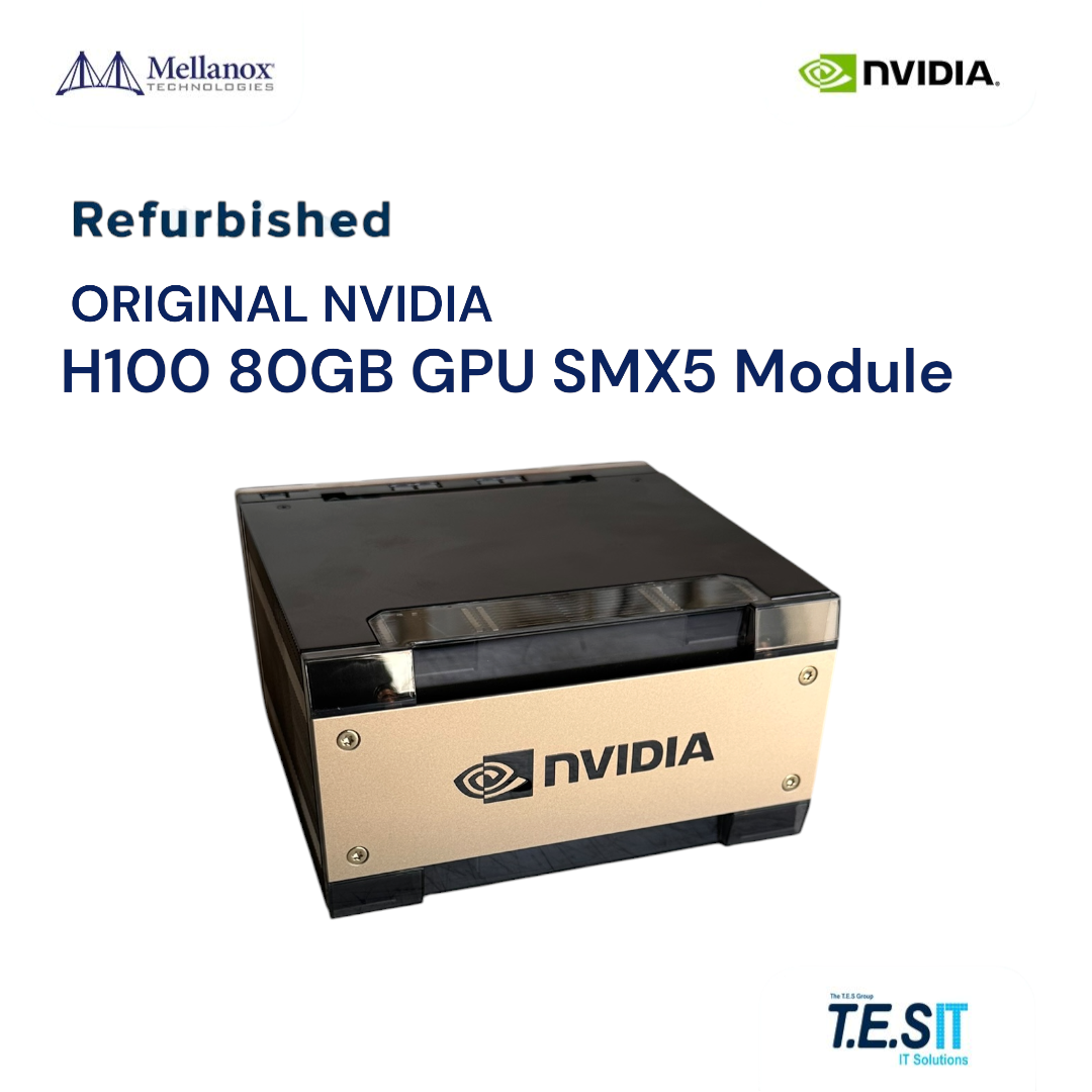

NVIDIA H100 80GB SXM5 — 699-2G520-0200-400 - GH100-885KK-A1
Hopper-architecture data-center GPU module built on GH100 silicon, die part number GH100-885KK-A1. 80 GB HBM3 at ~3.35 TB/s, 4th-gen Tensor Cores with FP8 Transformer Engine, 18 NVLink 4.0 links at 900 GB/s aggregate. Bare SXM5 mezzanine module for NVIDIA HGX H100 4-GPU and 8-GPU baseboards in DGX H100 and OEM HGX systems. Built for large-scale AI training, generative AI inference and HPC.
GPU Chip / Die Information
Factory laser marking on the exposed GH100 die of this module:
nVIDIA® / T TW 2221A1 / U8A629.0A2 (e1) / GH100-885KK-A1
- GPU die part number: GH100-885KK-A1 — Hopper GH100 die, SKU bin 885KK
- Silicon revision: A1 (production Hopper revision)
- Process: TSMC 4N
- Assembly / test origin: T TW — Taiwan
- Date code: 2221 = year 2022, work week 21
- Wafer lot / trace code: U8A629.0A2 — unique per production lot
- Package: bare die, no heat spreader; 80 GB HBM3 on-package, 5120-bit
The die code identifies the silicon only — not HBM3 capacity, module SKU, revision or OEM lock status. Those come from the module part number, the physical label and host software readout. T.E.S IT-SOLUTIONS certifies against the module part number and label, never the die marking alone.
Date code differences are normal. Modules in one HGX baseboard commonly carry different manufacturing weeks and lot codes, because OEMs populate baseboards from available inventory. This is not a sign of a counterfeit part, a repaired die or a performance difference.
Specifications
- Brand / MPN: NVIDIA 699-2G520-0200-400
- Type: Data-center GPU module, SXM5 mezzanine
- GPU silicon: GH100 Hopper, TSMC 4N — die PN GH100-885KK-A1, rev A1
- Memory: 80 GB HBM3, 5120-bit, ~3.35 TB/s
- Host interface: PCIe Gen 5 x16
- GPU-to-GPU: 4th-gen NVLink, 18 links, 900 GB/s
- Peak: FP64 60 · TF32 989 · BF16/FP16 1979 · FP8 3958 TFLOPS (2:4 sparsity)
- TDP: up to 700 W
- Features: FP8 Transformer Engine, NVLink 4, 2nd-gen MIG, Confidential Computing, DPX
- Condition: Refurbished — bench-tested by T.E.S IT-SOLUTIONS
What This Is NOT
- Not a PCIe card — SXM5 seats into an HGX baseboard socket. For PCIe servers use H100 PCIe or H100 NVL.
- Not bundled with baseboard, NVSwitch, heatsink or cooling — bare module only.
- Not a workstation GPU — no display outputs, headless compute only.
- Not an H200 or H100 NVL — H200 is 141 GB HBM3e; NVL is the 94 GB PCIe twin-board.
- Not Mellanox networking — this is a Hopper GPU, not ConnectX, BlueField, Spectrum or Quantum.
- Not identified by die marking alone — GH100-885KK-A1 is the silicon code, not the product SKU.
Compatibility
- Baseboards: Supermicro SYS-821GE-TNHR, Dell XE9680, HPE Cray XD670, Lenovo SR675 V3, Gigabyte G593-SD0, ASUS ESC N8-E11, Inspur NF5688G7
- DGX H100: field swaps via NVIDIA Enterprise Support only
- Host CPU: Intel Xeon 4th/5th Gen or AMD EPYC 9004/9005, PCIe Gen 5
- Software: CUDA 12.x, driver R525+, cuDNN 8.9+, NCCL 2.18+, TensorRT 9+
- Cooling: 700 W needs high-CFM HGX chassis or DLC cold plate
- Thermal: bare-die — heatsink mates directly to silicon; TIM to OEM spec
- Power: via HGX baseboard — no 12VHPWR or EPS12V on the module
- Networking: pairs with ConnectX-7 NDR or BlueField-3
FAQ
What does GH100-885KK-A1 mean? GH100 = Hopper compute die, 885KK = NVIDIA internal die SKU code, A1 = silicon revision. Silicon identity only — use the module part number for procurement, warranty and RMA.
How do I read the date code? Year plus manufacturing work week. On this unit 2221 = 2022, week 21. U8A629.0A2 is the wafer lot and trace code, unique to each production lot.
My other modules show a different date code — is that a problem? No. Modules with the same die part number and revision are functionally identical regardless of manufacturing week. Compatibility is set by module part number and VBIOS / NVSwitch firmware level.
Does a unique lot code mean the GPU was repaired or re-marked? No — lot codes differ on every module by design. Real warning signs are cracked or chipped silicon, tooling marks, inconsistent laser marking, or software serials that do not match the module label. We check all of these before shipping.
The die is bare with thermal compound on it — is that normal? Yes. SXM5 has no heat spreader, so residual compound on a pulled module is expected. Every module is cleaned, inspected under magnification for cracks, and given fresh TIM to OEM specification.
What condition is supplied? Refurbished. Visually inspected, die marking recorded and photographed, VBIOS read, TIM renewed, bench-tested where HGX topology is available — CUDA sanity, ECC check, thermal readout.
Why buy from T.E.S IT-SOLUTIONS
Europe-based data-center networking and accelerated-computing specialist serving HPC, AI and enterprise procurement since 2007. Every H100 module is identified by module P/N, GH100 die part number, silicon revision, date code and wafer lot code before shipping, and ships with a written TES QA record plus die-marking photographs. Free pre-sale compatibility advice for HGX baseboard, NVSwitch, CPU host and InfiniBand or Ethernet fabric pairing. EU stock, multi-currency B2B invoicing, worldwide express, direct engineering contact — not a call-centre.